|
|
|
|
|
|
| Silicon nanowires fabricated using an imprinting technology could be the way of the future for transistor-based biosensors. |
TSUKUBA, Japan, Feb 28, 2017 - (ACN Newswire) - Korean researchers are improving the fabrication of transistor-based biosensors by using silicon nanowires on their surface.
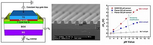 | | [Left] Schematic of a DG FET, [middle] SEM image of a cross-section of SiNWs fabricated on a silicon-on-insulator wafer and [right] change in the response voltage of planar and SiNW pH sensors for a wide range of pH (3–10). (c)2016 Cheol-Min Lim, In-Kyu Lee, Ki Joong Lee, Young Kyoung Oh, Yong-Beom Shin and Won-Ju Cho. |
The team, led by Won-Ju Cho of Kwangwoon University in Seoul, based their device on the 'dual-gate field-effect transistor' (DG FET).
When molecules bind on a field-effect transistor, a change happens in the surface's electric charge. This makes FETs good candidates for detecting biological and chemical elements. Dual-gate FETs are particularly good candidates because they amplify this signal several times. But they can still be improved.
The team used a method called 'nanoimprint lithography' to fabricate silicon nanowires onto the surface of a DG FET and compared its sensitivity and stability with conventional DG FETs.
Field-effect transistors using silicon nanowires have already been drawing attention as promising biosensors because of their high sensitivity and selectivity, but they are difficult to manufacture. The size and position of silicon nanowires fabricated using a bottom-up approach, such as chemical vapor deposition, cannot always be perfectly controlled. Top-down approaches, such as using an electron or ion beam to draw nanorods onto a surface, allow better control of size and shape, yet they are expensive and limited by low throughput.
Cho and his colleagues fabricated their silicon nanowires using nanoimprint lithography. In this method, a thin layer of silicon was placed on top of a substrate. This layer was then pressed using a nanoimprinter, which imprints nano-sized wire-shaped lines into the surface. The areas between separate lines were then removed using a method called dry etching, which involves bombarding the material with chlorine ions. The resultant silicon nanowires were then added to a DG FET.
The team found that their device was more stable and sensitive than conventional DG FETs. "We expect that the silicon-nanowire DG FET sensor proposed here could be developed into a promising label-free sensor for various biological events, such as enzyme-substrate reactions, antigen-antibody bindings and nucleic acid hybridizations [a method used to detect gene sequences]," conclude the researchers in their study published in the journal Science and Technology of Advanced Materials.
Article information
Cheol-Min Lim, In-Kyu Lee, Ki Joong Lee, Young Kyoung Oh, Yong-Beom Shin and Won-Ju Cho.
Improved sensing characteristics of dual-gate transistor sensor using silicon nanowire arrays defined by nanoimprint lithography.
Science and Technology of Advanced Materials, 2016; 18:1, 17-25.
http://dx.doi.org/10.1080/14686996.2016.1253409
For further information please contact:
Professor Won-Ju Cho*,
Department of Electronic Materials Engineering, Kwangwoon University, Korea
*E-mail: chowj@kw.ac.kr
Journal information
Science and Technology of Advanced Materials (STAM), http://www.tandfonline.com/STAM) is an international open access journal in materials science. The journal covers a broad spectrum of topics, including synthesis, processing, theoretical analysis and experimental characterization of materials. Emphasis is placed on the interdisciplinary nature of materials science and on issues at the forefront of the field, such as energy and environmental issues, as well as medical and bioengineering applications.
For more information about STAM contact
Mikiko Tanifuji
Publishing Director
Science and Technology of Advanced Materials
E-mail: TANIFUJI.Mikiko@nims.go.jp
Press release distributed by ResearchSEA for Science and Technology of Advanced Materials.
Topic: Research and development
Source: Science and Technology of Advanced Materials
Sectors: Materials & Nanotech, BioTech
https://www.acnnewswire.com
From the Asia Corporate News Network
Copyright © 2026 ACN Newswire. All rights reserved. A division of Asia Corporate News Network.
|
|
|
|

|
|
|
|