|
|
|
|
|
|
- New technology overcomes issues of existing metallic inks and enables low-resistance wire formation using low-temperature process at less than 100 degrees Celsius
- Vacuum-less and resist-less direct wire formation on numerous surfaces including PET film and glass achieved |
TOKYO, May 31, 2017 - (ACN Newswire) - Tanaka Holdings Co., Ltd. (head office: Chiyoda-ku, Tokyo; Representative Director & CEO: Akira Tanae) announced today that Electroplating Engineers of Japan, Ltd. (EEJA; plant and office: Hiratsuka City, Kanagawa Prefecture; Representative Director & CEO Muneharu Nakanouchi) used surface treatment chemicals (photosensitive primer used with a colloid catalyst) that it developed to create a new direct patterning plating technology. This technology does not require a vacuum environment or photoresist(*1), and can directly form low-resistance fine wires on a variety of materials using a low-temperature process that can be performed at or below 100 degrees Celsius.
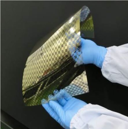 | | Au wires formed on PET film |
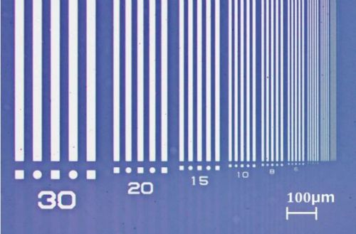 | | Wires ranging from 30 um to 5 um in width formed using the new technology |
 |
The new technology is a plating technique whereby a photosensitive primer is applied to various substrates such as PET film or glass and exposed to light; after the substrate is immersed in a colloid catalyst solution that includes a gold nanoparticle(*2) catalyst. The catalyst is immersed in a electroless plating solution(*3) with whatever metal that has been selected for the specific application to form fine electronic circuitry patterns made of various metals with a wire width of 5 um (a micrometer is one-millionth of a meter). Recently, metallic inks have been a focus of attention as a next-generation metal wire formation technology, but this new technology is able to create low-resistance wires using a lower temperature process compared to the wire formation process used for existing metallic inks. In addition, a groundbreaking method of automatic adsorption of the gold nanoparticle catalyst by the photosensitive primer makes it possible to directly form the wires without using a photoresist. The new technology forms wires using a plating method that does not require vacuum equipment, facilitating the expansion to large batch processing(*4), which will make it possible to form high-performance metallic wires on various substrates and enable mass production.
As a result of the characteristics and benefits of this technology, it is expected to open new areas of next generation electronics processes that could not be achieved with existing metal wire forming technologies.
Main Features of the New Technology
- Produces wires with much lower volume resistivity (Au: 3.3 uohm-cm, Cu: 2.3 uohm-cm) using a low-temperature process at or below 100 degrees Celsius
- Directly forms fine wires on a variety of non-conductive materials including PET film and glass
- Does not require a vacuum environment or photoresist
Examples of Wire Formation Using the New Technology
(Images)
- Au wires formed on PET film http://bit.ly/2sh4mW1
- Wires ranging from 30 um to 5 um in width formed using the new technology http://bit.ly/2qvcW7a
Newly-developed photosensitive primer and colloid catalyst surface treatment chemicals
When developing the new technology, EEJA independently developed a photosensitive primer and a colloid catalyst as new surface treatment chemicals.
- Photosensitive Primer
The photosensitive primer is an application-type resin solution based on organic solvents and is used to supplement the gold nanoparticle catalyst on the substrate. By exposing the photosensitive primer to ultraviolet light, the ability to supplement the gold nanoparticles are eliminated in areas other than where wires are to be formed.
- Colloid catalyst
The colloid catalyst is a water solution that includes a gold nanoparticle catalyst and is automatically absorbed onto the priming paint surface. The gold nanoparticle catalyst has high catalytic activity in various types of electroless plating solutions, and as a result, a precipitation reaction occurs in the metal from adsorption in the electroless plating solution.
Issues with existing technologies
There has been strong demand in recent years for development of vacuum-less and resist-less metal wire formation technologies exemplified by printed electronics(*5) as core technologies of next generation electronics. Furthermore, development of metallic inks has become active as a leading candidate for a next-generation wire formation technology. Research that will enable the formation of wires with lower resistance at lower temperatures is being conducted, but it has not been possible to achieve both low-temperature wire formation and low-resistance wires. EEJA developed this new technology based on the idea that a plating method that deposits metallic crystals from a water solution at under 100 degrees Celsius will make it possible to form low-resistance wires using a low-temperature process.
Benefits of the new technology
- Vacuum-less and resist-less fine-wire formation
The new technology is centered on plating techniques and forms wires from a water solution, and consequently, a vacuum environment is not needed. By using a groundbreaking method of automatic adsorption of the gold nanoparticle catalyst by the photosensitive primer, direct wire formation is possible without the use of a photoresist. Expansion for large batch processing will be easy, making it possible to form high-performance metallic wires on various substrates and enabling mass production.
- Formation of low-resistance wires is possible using a low-temperature process
This technology uses a low-temperature process at under 100 degrees Celsius to produce wires with much lower volume resistivity (Au: 3.3 uohm-cm, Cu: 2.3 uohm-cm) compared to existing metallic ink technologies. As a result, it is possible to form high-performance wires on non-conductive materials with low temperature resistance such as PET and other general-purpose plastic films.
- Adequate bonding strength on smooth substrates
Wire formation that exhibits adequate bonding strength (0.5 N/mm) even on smooth-surface PET film (Ra = 10 nm) is possible. Surface roughing of the substrate is not needed, and high adhesion is achieved.
- Light exposure that does not require nitrogen purging or ozone elimination
The wavelength of the ultraviolet radiation to which the primer is exposed is in the range of 300 nm, and therefore, it is not necessary to use the short wavelength excimer UV light (with a wavelength of 200 nm or shorter) that is used with existing pattern wire formation technologies that modify the substrate surface. This means that external utilities such as nitrogen purging and ozone elimination from the light source are not needed.
- Application to a variety of printing processes is possible
Wire formation using printing processes that employ methods such as partial printing of the colloid catalyst solution with the primer applied to the substrate surface or printing primer on the substrate and immersing in a colloid catalyst solution are possible. As a result, the technology can be applied to various wire formation techniques that combine printing methods and light exposure methods.
Examples of application and possibilities of the new technology for new-generation electronics
The new technology can form low-resistance, fine wires at low temperature, and its main applications are expected to be flexible displays, antennas, and sensors. Formation of fine wires on three-dimensional surfaces is a possibility, and consequently, application to molded interconnect devices (MID; molded resin components with integrated wiring and electrodes) may be possible. In addition, multilayer wiring formation has successfully been achieved by combining application-type insulation materials, and there are expectations that this technology will lead to innovations in metal wire formation technology.
EEJA plans to begin sample shipments of the photosensitive primer, colloid catalysts, and electroless plating solution used with this technology by end of this year.
This technology won the "JPCA Show Award" at the JPCA Show 2017 (47th Japan Electronics Packaging and Circuits Association Show), which will be held from June 7 to 9 of this year. EEJA will display this technology at its booth and will have a special panel display at 7H-29 in East Hall 5 during the show.
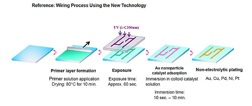
Reference: Wiring Process Using the New Technology
(Image: http://bit.ly/2rzZMpM)
(1) Primer layer formation: The primer is applied to the substrate and dried for several minutes at 80 degrees Celsius to 150 degrees Celsius to form an acceptor on the primer surface to capture the gold nanoparticles.
(2) Exposure: A photomask is used to expose the substrate to ultraviolet light for 10 to 60 seconds. The capture ability of the acceptor on the areas of the primer surface that are exposed to the ultraviolet light is eliminated.
(3) Au nanoparticle catalyst adsorption: After exposure, the substrate is immersed for 10 to 600 seconds in a colloid solution that includes gold nanoparticles, which have the ability to be adsorbed by the acceptor. The gold nanoparticles in the colloid solution adhere to the acceptor on the primer surface.
(4) Immersion in electroless plating solution: The substrate is immersed in a electroless plating solution of the type of metal to be formed into wires, and the metal in the plating solution is deposited along the gold nanoparticles fixed on the primer surface, forming the metal pattern.
*1 Photoresist
A photosensitive, corrosion-resistant film. Photoresist is used when performing photo etching, which employs photography technology and chemical corrosion (etching) to perform detailed processing of metals, semiconductors, and other materials.
*2 Gold nanoparticles
Gold particles on the nanometer scale (one-billionth of a meter).
*3 Electroless plating solution
A plating solution that causes reduction precipitation of metallic ions as metal on a substrate material through a chemical reaction between the metallic ions and a reducing agent.
*4 Large-batch processing
Large surface processing, simultaneous multi-board processing, and other processes characterized by plating techniques.
*5 Printed electronics
Technology for forming electronic circuits, devices, and so on using printing technology.
Press release: http://www.acnnewswire.com/clientreports/598/2017531_EN.pdf
Tanaka Holdings Co., Ltd. (Holding company of Tanaka Precious Metals)
Headquarters: 22F, Tokyo Building, 2-7-3 Marunouchi, Chiyoda-ku, Tokyo
Representative: Akira Tanae, Representative Director & CEO
Founded: 1885
Incorporated: 1918*
Capital: 500 million yen
Employees in consolidated group: 3,476 (as of March 31, 2016)
Net sales of consolidated group: 1,026.7 billion yen (FY2015)
Main businesses of the group: Strategic and efficient group management and management guidance to group companies as the holding company at the center of the Tanaka Precious Metals.
Website:
http://www.tanaka.co.jp/english (Tanaka Precious Metals), http://pro.tanaka.co.jp/en (Industrial products)
* Tanaka Holdings adopted a holding company structure on April 1, 2010.
Electroplating Engineers of Japan Ltd. (EEJA)
Head office: 5-50 Shinmachi, Hiratsuka-shi, Kanagawa
Representative: Muneharu Nakanouchi, Representative Director & CEO
Established: 1965
Capital: 100 million yen
Employees: 123 (FY2015)
Sales: 22,252.55 million yen (FY2015)
Areas of Business:
1. Development, production, sales and export of precious metal and base metal plating solutions, additives, and surface processing-related chemicals
2. Development, production, sales, and export of plating equipment
3. Import and sales of plating-related products
Website: http://www.eeja.com/en/index.html
About the Tanaka Precious Metals
Since its foundation in 1885, the Tanaka Precious Metals group has built a diversified range of business activities focused on precious metals. Tanaka is a leader in Japan in terms of the volumes of precious metals handled. Over the course of many years, Tanaka Precious Metals has not only manufactured and sold precious metal products for industry, but also provided precious metals in such forms as jewelry and resources. As precious metals specialists, all Group companies within and outside Japan work together with unified cooperation between manufacturing, sales, and technological aspects to offer products and services. In addition, in order to make further progress in globalization, Tanaka Kikinzoku Kogyo welcomed Metalor Technologies International SA as a member of the Group in 2016.
As precious metal professionals, Tanaka Precious Metals will continue to contribute to the development of an enriching and prosperous society.
The five core companies in the Tanaka Precious Metals are as follows.
- Tanaka Holdings Co., Ltd. (pure holding company)
- Tanaka Kikinzoku Kogyo K.K.
- Tanaka Denshi Kogyo K.K.
- Electroplating Engineers of Japan, Limited
- Tanaka Kikinzoku Jewelry K.K.
Press inquiries
Tanaka Holdings Co., Ltd.
https://www.tanaka.co.jp/en/protanaka/inquiry/index.php
Topic: Press release summary
Source: TANAKA PRECIOUS METAL GROUP Co., Ltd.
Sectors: Metals & Mining, Electronics
https://www.acnnewswire.com
From the Asia Corporate News Network
Copyright © 2026 ACN Newswire. All rights reserved. A division of Asia Corporate News Network.
|
|
|
|

|
|
|
|


