|
|
|
|
|
|
(A Result of NexTEP: Joint Industry-Academia Practical Application Development Project)
Key Points
- Problems with sensor electrode materials in electrostatic capacity-type touch panels used in smartphones resulted in difficulties responding to increasing trends for three-dimensional curves, flexibility, and larger screens on displays.
- Tanaka Kikinzoku Kogyo constructed a system for manufacturing an almost invisible ultrafine wire metal mesh (MM) sensor film at a low cost, utilizing roll-to-roll process printing using silver nano ink.
- This means that touch panel functions can be added evenly to bendable displays and can be used in OLED displays. It is also anticipated that films with antibacterial, catalyst and thermal insulation functions will come into use. |
TOKYO, Jan 17, 2018 - (ACN Newswire) - JST (President, Michinari Hamaguchi) has recognized the results of NexTEP's project, "A Sensor Film for Touch Panels*1 Using Thin Metallic Wire" as a success.
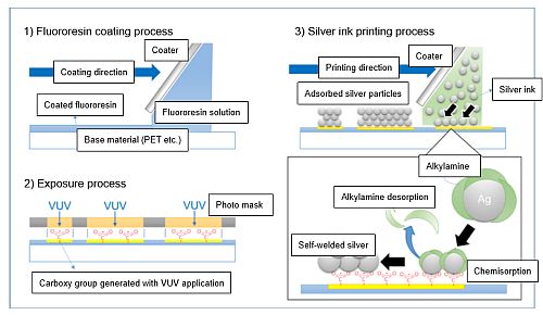 | | Figure 1. New technology (SuPR-NaP method) manufacturing processes and printing reaction mechanism |
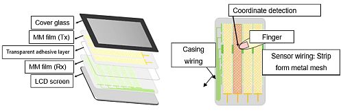 | | Figure 2. Metal mesh electrostatic capacity touch panel structure |
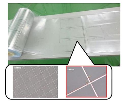 | | Figure 3. Sensor film continuously manufactured with the roll-to-roll method (7-inch pattern) |
This development task was based on the research of Professor Tatsuo Hasegawa, Principal Research Manager at the Flexible Electronics Research Center of the National Institute of Advanced Industrial Science and Technology, and was consigned to Tanaka Kikinzoku Kogyo (Representative Director & CEO, Akira Tanae, Chiyoda-ku, Tokyo) from April 2014 through September 2017. The research proceeded with the aim of practical application through Tanaka Kikinzoku Kogyo's Global Marketing/R&D Division.
In conventional electrostatic capacity-type touch panels*2, indium tin oxide (ITO) is used for the sensor. However, because of its high electrical resistivity and weakness upon bending, companies faced difficulties in increasing the size of such sensors and making them more flexible. Metal mesh*3 (MM) solves these problems, but it is difficult to make thinner than 4 um, and no technology existed to manufacture the mesh via printing.
To apply the new technology (SuPR-NaP method*4), which fabricates wiring through an adsorption reaction between special silver ink and an activated fluororesin surface, at a suitable speed for commercial manufacturing, the project clarified the reaction mechanism and researched the development of manufacturing equipment as well as the conditions for each process. As a result, the project constructed a system for manufacturing MM film (line width: 2-4 um) with the full process roll-to-roll method*5. In a 200,000-frequency (radius: 2 mm) bending test, this MM film exhibits hardly any changes in resistance values, and it has cleared general reliability testing.
This success in manufacturing the world's first micro-wiring film with a full process roll-to-roll method is an important technological innovation in printed electronics for the flexible electronic device market. It is also anticipated that the technology could be applied and used for applications requiring metal patterns on resin film (function films e.g. antibacterial, catalyst, thermal insulating).
Context
With the increased use of information technology in society, people are demanding access to information in various locations, at various times and in various situations. Touch panels that are integrated with the display are used in many devices, from smartphones, notebooks, large panel to automotive displays.
Moreover, touch sensors now need to be compatible with not only flat panel displays, but also recently-announced three-dimensional curved and bendable displays. Transparent (conducting) electrodes using ITO are mainly used for current touch sensors. However, physical problems such as high electrical resistivity and weakness upon bending imposed limitations on responding to needs for flexibility and increasingly large screen sizes. Metal mesh(MM), in which thin metallic wire is used as the electrode, is being applied on as a material that could solve these problems. However, as the line width and pitch of current MM is thick, the wiring is visible on smartphones, which are used at a short distance. Therefore, it has only come into popular use for large displays.
Development Details
With this new printing technology, a film to which liquid-repelling fluororesin is applied undergoes pattern exposure through a photo mask. Metal ink is then scanned onto it to form the wiring. This technology means that metal wiring with a fixed film thickness can be formed by means of the chemisorption of metal nanoparticles on the fluororesin surface activated by light.
The following technology has been developed to make it possible to manufacture MM film with micro wiring that can also be used for smartphones at a low cost. The project constructed a roll-to-roll production system that has not been available with existing manufacturing methods.
- The reaction mechanism for printing was elucidated, ink and fluororesin which was investigated and a method of even printing on large areas was developed. This made it possible to fabricate a 7- to 8-inch sensor film with micro wiring (line width: 2-4 um).
- Invisible wiring was developed by postprocessing the sensor pattern design (line width and shape) to respond to market needs. As a result, a MM film that could also be used for smartphones was able to be developed. The ability of this film to withstand 200,000-frequency (radius: 2 mm) bending test was also confirmed.
- Equipment for each process was developed and a manufacturing method with the roll-to-roll process was established. In a manufacturing experiment for the line width 4 um MM film, the 10m roll length achieved more than a 95% yield rate was achieved.
Anticipated Effects
This successful development is expected to enable the low-cost manufacturing of high-functioning touch panel sensor films that can be used for three-dimensional curved or bendable displays.
This manufacturing of a micro wiring film with full process roll-to-roll process is the first of its kind in the world. It is a breakthrough technological innovation for printed electronics used in the flexible electronic device market. It is anticipated that this technology can be not only applied and used in electronics fields such as OLED*6 displays, IoT device wiring and electrodes, but also in the manufacturing of functional films such as antibacterial films, films for catalysts and thermal insulation films.
Reference
Figure 1. New technology (SuPR-NaP method) manufacturing processes and printing reaction mechanism
https://www.acnnewswire.com/topimg/Figure1.jpg
1) Fluororesin application: Fluororesin that can repel silver ink is used to coat the base (PET film).
2) Exposure: When VUV*7 light is applied to the fluororesin surface, a carboxy group is formed. This property is used to form a carboxy group on the film in accordance with the photo mask pattern.
3) Silver nanoparticle printing: When the film is coated with silver ink after exposure, the silver nanoparticles undergo chemisorption onto the carboxy group alone. Excessive silver ink is removed by the coater (equipment used to spread out the applied liquid with a blade and scrape off excess liquid). Alkylamine, which had inhibited the aggregation of silver nanoparticles in the silver ink, is completely removed from the silver surface by postprocessing so that silver nanoparticles can fuse to each other. This makes it possible to form silver wiring with regular thickness.
Figure 2. Metal mesh electrostatic capacity touch panel structure
https://www.acnnewswire.com/topimg/Figure2.jpg
When a finger approaches the touch panel, electrostatic capacity created between vertical and horizontal sensor wiring and the finger is detected and the finger position coordinate is identified. Simultaneous detection of multiple points is also possible. With this technology, metal mesh is used in the sensor wiring. Normally, ITO is used.
Figure 3. Sensor film continuously manufactured with the roll-to-roll method (7-inch pattern)
https://www.acnnewswire.com/topimg/Figure3.jpg
Keywords
*1 Sensor film for touch panels
As shown in Figure 2, this is a film in which the mesh wiring is in strip form. Each piece of strip form mesh wiring is connected with the peripheral casing wiring and, the casing wiring is connected by the FPC cable.
*2 Electrostatic capacity-type touch panels
As shown in Figure 2, an electrostatic capacity touch panel is composed of two sensor films and a transparent adhesive sheet adhered on top of each other to form a layered structure. Because voltage is applied to the two sensors, the transparent adhesive layer between the sensor films has electrostatic capacity as a dielectric substance. Touch location sensing involves the detection of minute changes in electrostatic capacity that arise through finger proximity and contact. Simultaneous detection at multiple points is also possible. Although the principle upon which this is based is simple, the wiring pattern shape and controller IC detection algorithm have been adjusted in order to eliminate unintentional touches, noise, and temperature drift.
*3 Metal mesh
With this method, the wiring is composed of silver or copper wiring, rather than an ITO film. Because photolithography technology is used in the formation of um level wiring, low-cost manufacturing was considered to be difficult.
*4 SuPR-NaP method
In a substrate coated with liquid-repellant fluororesin, special silver nano ink reacts to a part that was modified with deep ultraviolet light. Then, silver nanoparticles undergo chemisorption so that the silver nanoparticles fuse to each other and form wiring.
*5 Full process roll-to-roll method
This refers to converting all manufacturing processes to roll-to-roll (print formation of circuits on rolled film substrates for production in roll format, allowing for the efficient production of electronic devices).
*6 OLED (Organic Light Emitting Diode)
This refers to an organic EL diode. Devices use the phenomenon whereby light is emitted when voltage is applied to certain types of organic compounds. Usage is expanding to lighting and displays.
*7 VUV (Vacuum Ultra Violet)
Vacuum ultraviolet light refers to using light with short wavelengths in region close to 10-200 nm in a vacuum atmosphere. Because light with wavelengths of 200 nm or below is absorbed by oxygen, etc., in the air, the optical path needs to be made into a vacuum during use.
Press release (PDF): http://www.acnnewswire.com/clientreports/598/201801.pdf
Press inquiries
Tanaka Holdings Co., Ltd.
https://www.tanaka.co.jp/en/protanaka/inquiry/index.php
Topic: Press release summary
Source: TANAKA PRECIOUS METAL GROUP Co., Ltd. / Japan Science and Technology Agency (JST)
Sectors: Metals & Mining, Electronics, Materials & Nanotech
https://www.acnnewswire.com
From the Asia Corporate News Network
Copyright © 2026 ACN Newswire. All rights reserved. A division of Asia Corporate News Network.
|
|
|
|

|
|
|
| |
| TANAKA PRECIOUS METAL GROUP Co., Ltd. Related News |
|
| Mar 20, 2026 20:00 HKT/SGT |
| TANAKA Announces Executive Appointments |
|
| Tuesday, 17 March 2026, 21:00 JST |
| TANAKA PRECIOUS METAL GROUP Provides Medals, Commemorative Items, and Trophies as Category Sponsor (Awards Ceremonies) for the LIGA.i Blind Soccer Top League 2025 |
|
| Mar 10, 2026 10:00 HKT/SGT |
| TANAKA PRECIOUS METAL TECHNOLOGIES 在各国同行企业中率先成功开发出在100度左右表现出更优异的氢透过性能的更高性能钯氢透过膜 |
|
| Thursday, 5 March 2026, 22:00 JST |
| TANAKA Develops World's First High-Performance Palladium Hydrogen Permeable Membrane Exhibiting High Hydrogen Purification Performance at Temperatures around 100 degrees C |
|
| Mar 5, 2026 10:00 HKT/SGT |
| TANAKA PRECIOUS METAL TECHNOLOGIES 确立了烧结金(Au)接合技术“AuRoFUSE(TM) Preforms”的转印技术 |
|
| More news >> |
|
|
|


