|
|
|
|
|
|
| New technologies allow for longer range, higher capacity wireless communications with lower power consumption |
TOKYO, July 24, 2017 - (JCN Newswire) - Fujitsu Limited and Fujitsu Laboratories Ltd. today announced the development of a gallium-nitride (GaN)(1) high-electron mobility transistor (HEMT)(2) power amplifier for use in W-band (75-110 GHz) transmissions.
 | | Figure 1: Schematic cross-sectional view of GaN-HEMT device structure |
 | | Figure 2: Comparison of transistor characteristics |
 | | Figure 3: Picture of the newly developed W-band GaN-HEMT power amplifier chip |
 | | Figure 4: Comparison of GaN-HEMT power amplifier performance |
To realize long-distance, high-capacity wireless communications, a promising approach is to utilize the W-band and other high frequency bands that encompass a broad range of usable frequencies, and increase output with a transmission power amplifier. At the same time, demand exists for improved efficiency in power amplifiers in order to mitigate the increased power consumption of communication systems.
Fujitsu has now succeeded in developing a power amplifier for use in W-band transmissions that offers both high output power and high efficiency, improving transistor performance through the reduction of electrical current leakage and internal GaN-HEMT resistance. Fujitsu has achieved 4.5 watts per millimeter of gate width, the world's highest output density in the W-band, and has confirmed a 26% reduction in energy consumption compared to conventional technology.
Fujitsu anticipates that setting this power amplifier between wireless communication systems in two locations will achieve high-bandwidth communications at 10 gigabits per second (Gbit/s) over a distance of 10km.
Part of this research was carried out with support from Innovative Science and Technology Initiative for Security, established by the Acquisition, Technology & Logistics Agency (ATLA), Japan Ministry of Defense.
Details of this technology will be announced at the 12th International Conference on Nitride Semiconductors (ICNS-12), to be held in Strasbourg, France, from July 24 until July 28th.
Development Background
Wireless data traffic from mobile communications has increased dramatically over the last few years, and with the spread of 5G and IoT devices it is predicted to increase at an annual growth rate of 1.5 times until the year 2020. In order to build this sort of high capacity next-generation wireless communications network, attention has been focused on wireless communication technology using the high frequency W-band. The range of frequencies that can be used in the W-band is very broad, and because communication speed can be rapidly increased in this band, it is well-suited for this kind of high bandwidth wireless communication.
Conventional wireless communications technology, has allowed for performance of several Gbit/s over distances of several kilometers, but achieving an even greater increase in wireless communication distance and capacity utilizing the W-band demands further increases to the output of power amplifiers to boost signals during transmission.
Issues
To increase distance and capacity, it will be necessary to expand the frequency bandwidth that can be amplified while simultaneously supporting modulation methods that can transmit more information within the same frequency bandwidth, and a strong requirement is to have less distortion when the signal is amplified. Another pursuit is keeping in check the energy consumption of communication systems that accompanies greater distances and capacities, and the improved energy efficiency in power amplifiers.
About the Newly Developed Technology
In order to both increase the distance and capacity of wireless communications and decrease energy consumption with indium-aluminum-gallium-nitride (InAlGaN) HEMTs, Fujitsu has developed two technologies that effectively reduce internal resistance and current leakage. Features of the newly developed technologies are as follows:
1. Technology to reduce internal resistance
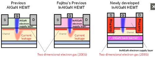
Fujitsu has developed device technology that can reliably reduce resistance to one tenth that of previous technology when current flows between the source or drain electrodes and the GaN-HEMT device. The technology utilizes a manufacturing process that embeds GaN plugs directly below the source and drain electrodes, which generate electrons at high densities (fig. 1).
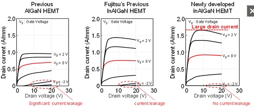
It is necessary to transport the electrons that come from the source electrode to the two dimensional electron gas field as smoothly as possible. The structure of the previous technology causes the electron supply layer to become a barrier, however, and internal resistance increases between the source electrode and the two dimensional electron gas. By applying this new technology, Fujitsu succeeded in running high currents through the transistor with significantly less resistance (fig. 2).
2. Technology to control current leakage
A current leakage occurs when the two dimensional electron gas, which moves at high speed on the boundary at the top of the channel layer, takes a detour below the gate when the transistor is in its off-state. This leakage causes deterioration in the operational performance of the power amplifier. Normally, it is possible to reduce current leakage by placing a barrier layer beneath the channel layer, but in that case the amount of two dimensional electron gas also decreases, and leads to a reduction of the drain current.
This new technology maintains high drain currents by effectively distributing indium-gallium-nitride (InGaN) to create a barrier layer below the channel layer. This reduces electron detours during operation, successfully providing significant reductions in current leakage (fig.1, fig. 2).
http://www.acnnewswire.com/topimg/Low_FujitsuTransmitter72417Fig1.jpg
Figure 1: Schematic cross-sectional view of GaN-HEMT device structure
http://www.acnnewswire.com/topimg/Low_FujitsuTransmitter72417Fig2.jpg
Figure 2: Comparison of transistor characteristics
Effects
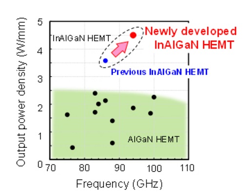
The previous world record for power amplifier output density in the W-band for transmitters was 3.6 watts per millimeter of gate width with technology developed by Fujitsu Laboratories. This has improved significantly with the newly developed technology, which delivers power output of 4.5 watts per millimeter of gate width for a power amplifier designed to operate at 94GHz. In addition, this new technology achieved a reduction in energy consumption of 26% compared to the previous technology through a reduction in current leakage. It is anticipated that the use of this power amplifier will allow the achievement of high capacity, long distance wireless communications between two connected systems at different locations at over 10Gbit/s and at distances greater than 10km.
http://www.acnnewswire.com/topimg/Low_FujitsuTransmitter72417Fig3.jpg
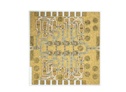
Figure 3: Picture of the newly developed W-band GaN-HEMT power amplifier chip
http://www.acnnewswire.com/topimg/Low_FujitsuTransmitter72417Fig4.jpg
Figure 4: Comparison of GaN-HEMT power amplifier performance
Future Plans
Fujitsu aims to apply this technology broadly to the development of power amplifiers for purposes that call for wireless communications that offer long range and higher capacity, while offering easier installation than fiber optics. The goal is to commercialize this technology in high speed wireless communication systems by 2020, with an aim to employ it in such situations as a method of restoring communications when fiber optic cables have been severed by natural disasters or as a way of setting up temporary communications infrastructure when holding events.
(1) Gallium nitride (GaN)
A wide band-gap semiconductor material that operates with a higher breakdown-voltage than semiconductor technologies based on previous materials, such as silicon (Si)- or gallium-arsenide (GaAs)-based technologies.
(2) High electron mobility transistor (HEMT)
A field-effect transistor that takes advantage of operation of the electron layer at the boundary between semiconductor materials with different bandgaps, which is relatively rapid compared to that within conventional semiconductors. Invented in 1980 by Fujitsu, this technology is currently used in a number of IT applications, including satellite transceivers, cellular equipment, GPS-based navigation systems, and broadband wireless networking systems.
About Fujitsu Laboratories
Founded in 1968 as a wholly owned subsidiary of Fujitsu Limited, Fujitsu Laboratories Ltd. is one of the premier research centers in the world. With a global network of laboratories in Japan, China, the United States and Europe, the organization conducts a wide range of basic and applied research in the areas of Next-generation Services, Computer Servers, Networks, Electronic Devices and Advanced Materials. For more information, please see: http://www.fujitsu.com/jp/group/labs/en/.
Contact:
Fujitsu Laboratories
Devices & Materials Laboratory
E-mail: next-press@ml.labs.fujitsu.com

Fujitsu Limited
Public and Investor Relations
Tel: +81-3-6252-2176
URL: www.fujitsu.com/global/news/contacts/
Topic: Press release summary
Source: Fujitsu Ltd
Sectors: Electronics
https://www.acnnewswire.com
From the Asia Corporate News Network
Copyright © 2024 ACN Newswire. All rights reserved. A division of Asia Corporate News Network.
|
|
|
|

|
|
|
|
