|
|
|
|
|
|
| "POSFER-E series", approx. 40% less in price, approx. 40% smaller in footprint, 150% higher in throughput compared with conventional one, is suited for "smartphone" volume production use. The launch of "POSFER-E series" coincides with the additional sales channel in the United States to further expand business in the entire US. |
TOKYO, July 8, 2013 - (ACN Newswire) - Tanaka Holdings Co., Ltd. (the holding company of Tanaka Precious Metals) today announced that Electroplating Engineers of Japan Ltd. (EEJA), which operates the Tanaka Precious Metals' plating business, has developed "POSFER-E Series", compact, highly-functional and fully-automated semiconductor wafer electroplating equipment at a competitive price and launched on July 5.
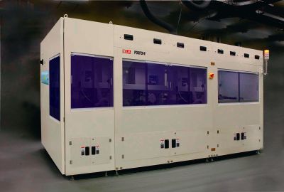 | | Electroplating Engineers of Japan (EEJA) has launched "POSFER-E series", which is compact, highly-functional and fully-automated electroplating semiconductor wafer equipment at a competitive price |
The "POSFER-E Series" is fully-automated semiconductor electroplating equipment for volume production of up to 8-inch wafers. In addition to its smaller footprint (3,400mm in width and 1,950mm in depth), "POSFER-E Series" has achieved 12,780 wafers per month throughput.
The price has been reduced by approx. 40% and its footprint reduced by approx. 40% while throughput has increased by approx. 150% compared to the POSFER-C Series (5,650mm in width, 2,000mm in depth, 8,500 wafers per month throughput). Furthermore, its unique cup structure capable of agitating the plating solution powerfully near the wafer surface, results in an improvement in embedding deep vias(*1) and thickness uniformity.
Semiconductor wafers up to 8 inches are used for smartphone components such as condensers, wireless LAN modules, bluetooth modules and memory and LEDs (light emitting diodes). Originally, the POSFER-C Series could be installed in a clean room, but as semiconductor manufacturing equipment has become smaller, it has become difficult to install large plating equipment.
Furthermore, the POSFER-C Series also presented the problem of being expensive due to the use of many parts to provide high productivity. In order to resolve these issues, EEJA has successfully developed the POSFER-E Series by fundamentally modifying the structure of the plating equipment such as reducing the number of cups by providing faster plating using a high current density, and adopting a dual arm robot to increase the efficiency of transportation. From July 5, a single plating type capable of forming a single layer of plating is sold as part of the lineup of the POSFER-E Series. Furthermore, in spring of 2014, a multi-plating type capable of forming two or more layers of plating is scheduled to be added to the POSFER-E Series and go on sale.
EEJA will sell the POSFER-E Series mainly in Japan and the United States, and aims for annual sales target of 1.2 billion yen. Moreover, in the future, an effort will be made to further expand the business by developing compact and fully-automated plating equipment for volume production of 12-inch semiconductor wafers.
New distributor is assigned in the United States to increase sales of plating equipment throughout America
To coincide with the launch of the POSFER-E Series, EEJA has concluded a distributor agreement with Tanaka Kikinzoku International K.K. (a subsidiary company of Tanaka Precious Metals; TKI), which handles import and exports sales of the Tanaka Precious Metals.
At the same time, a representative agreement was also concluded with Vacuum Engineering & Materials Co., Inc., (VEM) which has superior sales channels spanning throughout the entire United States, as a new representative for the sale of plating equipment in the United States. Upon sales, VEM will conduct marketing activities to customers and TKI will provide quotations and credit operations services. This will enable EEJA to expand its sales channels that were centered on the west coast even to the entire United States.
Until now, sales of EEJA plating equipment have been centered on customers in the west coast area where the semiconductor industry is thriving, but inquiries have been increasing from customers throughout the United States due to the growing demand of electronic components for smartphones. Because of this, EEJA has seen great growth potential in the entire United States, and decided to assign TKI and VEM as new distributors for its plating equipment.
In many cases, plating equipment manufacturers sell their plating equipment in the United States through distributors. EEJA, just like other manufactures, has concluded a representative agreement with Carmel Chemicals Inc. located at Santa Clara, California. Carmel Chemicals is a company performing sales activities based on the west coast area, and has made numerous sales of wafer bump plating equipment and plating equipment related to IC lead frames to large customers. In addition to Carmel Chemicals, EEJA also concluded agreements with TKI and VEM in order to expand sales of plating equipment to customers throughout the entire United States.
EEJA sells fully-automated electroplating equipment including the "POSFER Series" and semi-automated electroplating and electroless plating equipment in the United States. By adding TKI and VEM as plating equipment distributors, EEJA aims to increase sales in the United States six times by 2016.
EEJA will exhibit at SEMICON West 2013 to be held at the Moscone Convention Center in San Francisco, California for three days from July 9 (Tue) through July 11 (Thu). Technical staff will constantly be on-site in the exhibit booth 1619 to respond to interviews.
Press release: http://www.acnnewswire.com/clientreports/598/0708_EN.pdf
(*1) Via:
A fine through hole on a wafer or glass substrate to connect metal electrodes on the top and bottom layers of a chip as a miniaturization technology for semiconductor chips. Recently, vias diameter became smaller with around 10 to 20 micrometers, making it difficult for conventional cups to plate (fill) the inside of the vias with metal. The POSFER-E Series can plate deep vias with a small diameter by its cup structure capable of agitating the plating solution powerfully near the wafer surface.
Tanaka Holdings Co., Ltd. (Holding company of Tanaka Precious Metals)
Headquarters: 22F, Tokyo Building, 2-7-3 Marunouchi, Chiyoda-ku, Tokyo
Representative: Hideya Okamoto, President & CEO
Founded: 1885
Incorporated: 1918
Capital: 500 million yen
Employees in consolidated group: 3,869 (FY2011)
Net sales of consolidated group: 1.064 trillion yen (FY2011)
Main businesses of the group: Manufacture, sales, import and export of precious metals (platinum, gold, silver, and others) and various types of industrial precious metals products. Recycling and refining of precious metals.
Website: http://www.tanaka.co.jp/english
Electroplating Engineers of Japan Ltd. (EEJA)
Head office: 5-50 Shinmachi, Hiratsuka-shi, Kanagawa
Representative: Kazumasa Naito, President & CEO
Established: 1965
Capital: 100 million yen
Employees: 91 (FY2011)
Sales: 25,730 million yen (FY2011)
Areas of Business:
1. Development, production, sales and export of Sel-Rex precious metal and base metal plating
solutions, additives, and surface processing-related chemicals through a technical
partnership with the Enthone Group
2. Development, production, sales, and export of plating equipment
3. Import and sales of plating-related products
Website: http://www.eeja.com/
Tanaka Kikinzoku International K.K.
Headquarters: 22F, Tokyo Building, 2-7-3 Marunouchi, Chiyoda-ku, Tokyo
Representative: Tsuneo Sato, President & CEO
Founded: 1996
Incorporated: 1996
Capital: 470 million yen
Employees: 107 (FY2011)
Sales: 190.5 billion yen (FY2011)
Main businesses: Import, export and sales of various industrial products and manufacturing plants from Tanaka Precious Metals
Website: http://pro.tanaka.co.jp/en
Vacuum Engineering & Materials Co., Inc. (VEM)
Founded in 1987 originally as a materials brokerage, Vacuum Engineering & Materials Co., Inc. provided high purity metals to the Northern California semiconductor market. Manufacturing and stocking distribution of thin film materials followed for Semiconductor, Compound Semiconductor, Wireless RF & Microwave and etc.
Headquarters: 390 Reed Street Santa Clara, CA 95050 USA
Toll Free: +1-877-986-8900
Phone: +1-408-871-9900
Fax: +1-408-562-9125
E-mail: info[at]vem-co.com
Website: http://www.vem-co.com/
About the Tanaka Precious Metals
Established in 1885, the Tanaka Precious Metals has built a diversified range of business activities focused on the use of precious metals. On April 1, 2010, the group was reorganized with Tanaka Holdings Co., Ltd. as the holding company (parent company) of the Tanaka Precious Metals. In addition to strengthening corporate governance, the company aims to improve overall service to customers by ensuring efficient management and dynamic execution of operations. Tanaka Precious Metals is committed, as a specialist corporate entity, to providing a diverse range of products through cooperation among group companies.
Tanaka Precious Metals is in the top class in Japan in terms of the volume of precious metal handled, and for many years the group has developed and stably supplied industrial precious metals, in addition to providing accessories and savings commodities utilizing precious metals. As precious metal professionals, the Group will continue to contribute to enriching people's lives in the future.
The eight core companies in the Tanaka Precious Metals are as follows.
- Tanaka Holdings Co., Ltd. (pure holding company)
- Tanaka Kikinzoku Kogyo K.K.
- Tanaka Kikinzoku Hanbai K.K.
- Tanaka Kikinzoku International K.K.
- Tanaka Denshi Kogyo K.K.
- Electroplating Engineers of Japan, Limited
- Tanaka Kikinzoku Jewelry K.K.
- Tanaka Kikinzoku Business Service K.K.
Press inquiries
Global Sales Dept., Tanaka Kikinzoku International K.K. (TKI)
https://www.tanaka.co.jp/support/req/ks_contact_e/index.html
Topic: New Product
Source: TANAKA PRECIOUS METAL GROUP Co., Ltd.
Sectors: Metals & Mining, Electronics, Daily Finance
https://www.acnnewswire.com
From the Asia Corporate News Network
Copyright © 2026 ACN Newswire. All rights reserved. A division of Asia Corporate News Network.
|
|
|
|

|
|
|
|

