|
| Monday, 19 January 2015, 13:00 HKT/SGT | |
| |  | |
Source: NIMS | |
|
|
|
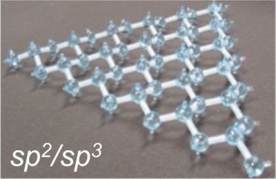
Nomi, Japan, Jan 19, 2015 - (ACN Newswire) - Silicene is the thinnest form of silicon. It is metallic, has graphene-like mobile carriers and can behave like a semiconductor. The wonder material could lead to even smaller electronics but challenges remain in this review published in the Science and Technology of Advanced Materials.
 | | Wonder Material Silicene Still Stands Just Out of Reach |
Scientists in Japan compared the properties of a hypothetical freestanding one-atom-thick layer of silicon to a similar sheet developed on a metal substrate. Although promising, this second "epitaxial" form shows important differences. Turning the hypothetical material into a reality still remains a major challenge, 20 years after it was first reported.
In 1994, scientists published their first theoretical report on the thinnest possible form of silicon. Among many other uses, silicon is incorporated as a semiconductor in integrated circuits, the basis of most computers.
But it was only ten years later in 2004, when another material, graphene, was reported, that scientists started showing a real interest, and eventually named the material, "silicene".
Graphene is a one-atom-thick layer of carbon that has been shown to host the fastest carriers of electricity yet found. Compared with silicon, however, graphene is not a semi-conductor because it can't switch between conducting and not conducting states. This makes it very difficult to apply it in a switching device such as a transistor.
This is why silicene is so exciting. In its freestanding form, this one-atom-thick layer of silicon atoms has graphene-like mobile carriers as well and is metallic. On the other hand, for instance by applying strain or an electric field, it could also be turned to behave like a semiconductor. This is because the structure could be easily modified or switched on the atomic scale. In addition, it would be compatible with already existing silicon-based circuitry. This is envisaged to lead to the development of even smaller electronics than those currently on the market.
Because of its exciting potential, the experimental demonstration of the existence of silicene was highly anticipated. In 2012, several groups reported successfully developing "epitaxial" silicene: silicene sheets formed on metallic substrates. A team of Japanese scientists compared the characteristic properties of theoretical freestanding silicene to epitaxial silicene they had produced on a zirconium diboride substrate. They found that the crystal structure of epitaxial silicene was strongly influenced by its metal substrate, thus resulting in electronic properties different from those predicted for the hypothetical freestanding form.
The synthesis of freestanding silicene remains a major challenge and many of the properties of its epitaxial form are not yet fully understood. However, the team of Japanese scientists joined by a few other groups worldwide will further work on the understanding of the formation mechanism of epitaxial silicene and its interaction with the substrate. Based on the deep understanding of this matter, present and future work is anticipated to result in the required developments such as the formation of silicene on an insulating platform and its successful encapsulation. This would then lead to practical applications of the material.
For further information contact:
Associate Professor Yukiko Yamada-Takamura
School of Materials Science
Japan Advanced Institute of Science and Technology
Nomi, Japan
Tel: +81-761-51-1570
E-mail: yukikoyt@jaist.ac.jp
More information about the research paper
Yukiko Yamada-Takamura and Rainer Friedlein 2014 Sci. Technol. Adv. Mater. 15 064404 doi:10.1088/1468-6996/15/6/064404
The paper is available for download from http://iopscience.iop.org/1468-6996/15/6/064404
Press release distributed by ResearchSEA for National Institute for Materials Science.
Topic: Research and development
Source: NIMS
Sectors: Science & Research
https://www.acnnewswire.com
From the Asia Corporate News Network
Copyright © 2026 ACN Newswire. All rights reserved. A division of Asia Corporate News Network.
|
|
|


