|
| Tuesday, 24 March 2015, 16:05 HKT/SGT | |
| |  | |
Source: ULVAC, Inc. | |
|
|
|
|
| - Developed for piezoelectric MEMS devices integrated on CMOS |
Chigasaki, Japan, Mar 24, 2015 - (ACN Newswire) - ULVAC, Inc. (hereafter referred to as ULVAC) today announced the industry's first* low temperature PZT sputtering technology in mass production scale, enabling future advanced MEMS devices integrated on CMOS which will be the mainstream of next generation MEMS devices.
 | | ULVAC Announces World's First, Low Temperature PZT Sputtering Technology in Mass Production Scale |
Background
Today many sensors such as accelerometers, gyros, and pressure sensors are widely used inside high performance smart phones, tablet PCs, and automobiles enabling the "Smart society" representing the IoT world. The increasing demand and the key element to enable this functionality, is the piezoelectric MEMS (Micro Electro Mechanical Systems) device, using a piezoelectric thin film material called PZT (lead zirconate titanate, Pb(Zr,Ti) O3). Examples of applications in use are: actuators for auto focus lenses on digital cameras, and inkjet heads for printers.
The future holds that, higher performance, multi-functional and smaller piezoelectric MEMS devices for the next generation of advanced sensor technology is rapidly expanding its applications by the integration with CMOS (Complementary Metal Oxide Semiconductor) devices. PZT, Piezo-electric MEMS is one of the most practical MEMS devices available today, however, the process temperature was an obstacle, to integrate the MEMS device directly onto a CMOS device. A CMOS device due to its nature, can only withstand a process temperature of 500 degrees C or lower. A typical crystallization temperature for a PZT thin film is 600 degrees C for sputtering and 700 degrees C for Sol-Gel.
ULVAC has developed world's first unique innovative technology allowing integration of the piezoelectric MEMS device onto a CMOS device, thus achieving highest level piezoelectric performance, withstand voltage reliability, and cycle performance. This is accomplished by utilizing unique sputtering technology with process temperature below 500 degrees C.
Insight of the Technology
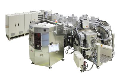
The piezoelectric device, using thin film PZT, is formed by five (5) layers which are: an adhesion layer, a lower electrode layer, a buffer layer, a piezoelectric (PZT) layer, and upper electrode layer. All the accumulated layers are formed sequentially, through one single sputtering system developed by ULVAC. This multi-chamber type sputtering system (model SME-200) allows for consistent process flow, optimizing each individual layer inside each process chamber respectively, achieving highly stable repeatability of the stacked layer performance, and also improving throughput, to that which is that is very suitable for mass production purposes.
Additionally this system is designed to achieve highly uniform and stable process utilizing 8-inch silicon wafers, the largest size substrate available for MEMS device mass production known today. Maximum seven (7) process chamber such as DC and RF magnetron sputtering chamber, RTA (Rapid Thermal Annealing) chamber to accelerate crystallization, and a load-lock chamber are utilized.
The PZT thin film is accumulated by crystal growth on a heated wafer. The sputtering chamber is specifically designed for dielectric material to allow stable deposition process and lead composition control, a character required for highly volatile materials such as PZT. The world's highest PZT thin film performance level, in mass production is enabled, utilizing a new, low temperature process under 500 degrees C, and ULVAC unique process technology, for applying a buffer layer.
Parameters verified are; piezoelectric constant (e31) - 17 C/m2 , dielectric strength voltage +/- 100V, cycle performance >10(11th) PZT thin film thickness of 2.0 um electrical performance.
Feature
1. Highly uniform and stable deposition technology on an 8 inch wafer scale utilizing specially designed sputtering chamber for dielectric materials.
2. High deposition rate and throughput in mass production scale for PZT thin film.
3. ULVAC unique and stable process allowing high performance PZT thin film in mass production scale under 500 degrees C.
4. Highly repeatable accumulation process of PZT thin film piezoelectric device is formed within one system in mass production scale.
Future prospects
This innovative technology should open the window to new electrode materials, substrates, and manufacturing process for higher performance, multi-function, and smaller MEMS devices where high PZT deposition temperature had previously limited its functions.
Today ULVAC is the leader in providing total solutions for MEMS device and confident our technology will contribute to enable the further development and growth of the IoT world, which require advanced, stand-alone sensors, energy harvesting devices, and micro robots applications.
* based by ULVAC research and comparison March 25, 2015
Full press release: http://www.ulvac.co.jp/en/information/20150325/
Contact:
ULVAC, Inc.
Advanced Electronics Equipment Division
Yutaka Nishiyama
Tel: 81-467-89-2139 / Fax: 81-467-89-2297
http://www.ulvac.co.jp/products_e/
http://www.ulvac.co.jp/
Topic: New Product
Source: ULVAC, Inc.
Sectors: Electronics
https://www.acnnewswire.com
From the Asia Corporate News Network
Copyright © 2026 ACN Newswire. All rights reserved. A division of Asia Corporate News Network.
|
|
|
|

|
|
|
| |
| ULVAC, Inc. Related News |
|
| Friday, 1 May 2026, 11:00 JST |
| ULVAC Establishes Japan-Based Production for Rare-Earth Magnet Vacuum Melting Furnaces |
|
| Thursday, 19 June 2025, 9:30 JST |
| ULVAC Continues Participation in "Lab-in-Fab" Project to Advance Piezoelectric MEMS Technology, Now Entering a New Phase |
|
| Thursday, 24 April 2025, 9:30 JST |
| ULVAC Develops Dilution Refrigerator for Quantum Computers |
|
| Friday, 21 March 2025, 10:30 JST |
| ULVAC Developing Next-Generation Dilution Refrigerator for Quantum Computing by 2026 |
|
| Thursday, 13 February 2025, 8:30 JST |
| ULVAC Develops Roll-to-Roll Lithium Deposition System, Unveiling at Battery Japan |
|
| More news >> |
|
|
|

