|
|
|
|
|
|
| Helping reduce experimentation costs and development lead times, and enabling early problem-solving on mass production lines |
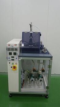
TOKYO, July 15, 2015 - (ACN Newswire) - Tanaka Holdings Co., Ltd. (Head office: Chiyoda-ku, Tokyo; Representative Director & CEO: Akira Tanae) today announced that Electroplating Engineers of Japan, Limited (Head Office: Hiratsuka-shi, Kanagawa; Representative Director & CEO: Koichiro Tanaka; EEJA), which operates the Tanaka Precious Metals' plating business, has developed, and launched from July 15, the RAD-Plater cup-type[1] ultra-compact plating laboratory equipment for semiconductor wafers, which achieves equivalent films to mass-production machines.
 | | Electroplating Engineers of Japan Launches Semiconductor Wafer Cup-type Ultra-compact Plating Laboratory Equipment on July 15 |
The RAD-Plater is ultra-compact laboratory equipment for manufacturing 2 to 8 inch semiconductor wafers. Measuring 800 mm wide and 700 mm deep, it is smaller than mass production machines and can operate on only compressed air and the 100 volt power of general equipment. In addition to gold, silver, palladium, copper and nickel, it can use a wide variety of plating solutions including alloys and lead-free solutions, and at 10 liters or less of solution, it uses about half the plating solution required by dip-type machines, which also reduces experimentation costs. The RAD-Plater uses an EEJA-manufactured Stir Cup[2] and delivers mass-production level plating quality through uniform and bubble-less film thickness and superior filling of deep vias[3]. It also enables reduced plating time by using a high current density[4] achieved with an increased ion supply. Even though the RAD-Plater is laboratory equipment, it achieves a level of plating equivalent to that of mass-production machines, which enables early problem-solving in the development stage for mass production issues such as expected yield, and enables trouble-free rollout to the mass-production line. This is the world's first cup-type plating laboratory equipment for manufacturing semiconductor wafers, using 10 liters or less of plating solution and handling 8-inch wafers.
Many development divisions of manufacturers with mass-production plating lines would have previously contracted out the plating solution experimentation work to equipment manufacturers and others for evaluation, but purchasing a RAD-Plater and conducting experiments in-house now enables a considerable reduction in development lead times. Other customers would have previously purchased mass-production machines to conduct their own experiments, but because the RAD-Plater comes at a cost that is one third to one quarter that of the mass-production machines, they can now achieve considerable cost reductions. EEJA provides samples of plating solution together with the RAD-Plater to research, development and trial manufacture divisions of manufacturers, universities and other education and research institutes, material manufacturers and others to improve sales of plating equipment and plating solutions for mass production. It aims to achieve RAD-Plater sales of 500 million yen per year by 2017.
Tanaka Precious Metals will be exhibiting at SEMICON West 2015 from July 14th to July 16th at the Moscone Center in San Francisco. Our engineers will be available to answer questions anytime at Booth No. 1628, South Hall.
[1] Cup-type
A specification of equipment for manufacturing semiconductor wafers, using a jet stream of plating solution and agitation to form a film. Another method is dip-type, which immerses the material to be plated. The trend in current plating processes is to use cup-type equipment for wafers of up to 8 inches and dip-type equipment for wafers of 12 inches or greater.
[2] Stir Cup
Random agitation of the solution on the plating surface of wafers improves ion supply uniformity and film thickness uniformity. It also produces pressure differentials in holes in the plating surface to continuously replenish the solution, which prevents bubbles from sticking to the plating surface and improves bubble removal.
[3] Via
A fine through-hole on a wafer or glass substrate to connect metal electrodes on the top and bottom layers of a chip, used as a miniaturization technology for semiconductor chips. Via diameters have recently become smaller, at around 10 to 20 micrometers, making it difficult for conventional plating cups to plate (fill) the inside of the vias with metal.
[4] Current density
Current density has been increased to 1.6 A/dcm2 from the 0.4 A/dcm2 of conventional laboratory equipment.
Press release: http://www.acnnewswire.com/clientreports/513/150715_EN.pdf
Tanaka Holdings Co., Ltd. (Holding company of Tanaka Precious Metals)
Headquarters: 22F, Tokyo Building, 2-7-3 Marunouchi, Chiyoda-ku, Tokyo
Representative: Akira Tanae, Representative Director & CEO
Founded: 1885
Incorporated: 1918
Capital: 500 million yen
Employees in consolidated group: 3,511 (FY2014)
Net sales of consolidated group: 856.4 billion yen (FY2014)
Main businesses of the group: Manufacture, sales, import and export of precious metals (platinum, gold, silver, and others) and various types of industrial precious metals products. Recycling and refining of precious metals.
Website: http://www.tanaka.co.jp/english (Tanaka Precious Metals), http://pro.tanaka.co.jp/en (Industrial products)
Electroplating Engineers of Japan Ltd. (EEJA)
Head office: 5-50 Shinmachi, Hiratsuka-shi, Kanagawa
Representative: Koichiro Tanaka, Representative Director & CEO
Established: 1965
Capital: 100 million yen
Employees: 95 (FY2014)
Sales: 22,480 million yen (FY2014)
Areas of Business:
1. Development, production, sales and export of precious metal and base metal plating solutions, additives, and surface processing-related chemicals
2. Development, production, sales, and export of plating equipment
3. Import and sales of plating-related products
Website: http://www.eeja.com/
About the Tanaka Precious Metals
Established in 1885, the Tanaka Precious Metals has built a diversified range of business activities focused on the use of precious metals. On April 1, 2010, the group was reorganized with Tanaka Holdings Co., Ltd. as the holding company (parent company) of the Tanaka Precious Metals. In addition to strengthening corporate governance, the company aims to improve overall service to customers by ensuring efficient management and dynamic execution of operations. Tanaka Precious Metals is committed, as a specialist corporate entity, to providing a diverse range of products through cooperation among group companies.
Tanaka Precious Metals is in the top class in Japan in terms of the volume of precious metal handled, and for many years the group has developed and stably supplied industrial precious metals, in addition to providing accessories and savings commodities utilizing precious metals. As precious metal professionals, the Group will continue to contribute to enriching people's lives in the future.
The eight core companies in the Tanaka Precious Metals are as follows.
- Tanaka Holdings Co., Ltd. (pure holding company)
- Tanaka Kikinzoku Kogyo K.K.
- Tanaka Kikinzoku Hanbai K.K.
- Tanaka Kikinzoku International K.K.
- Tanaka Denshi Kogyo K.K.
- Electroplating Engineers of Japan, Limited
- Tanaka Kikinzoku Jewelry K.K.
- Tanaka Kikinzoku Business Service K.K.
Press inquiries
Global Sales Dept., Tanaka Kikinzoku International K.K. (TKI)
https://www.tanaka.co.jp/support/req/ks_contact_e/index.html
Topic: New Product
Source: TANAKA PRECIOUS METAL GROUP Co., Ltd.
Sectors: Metals & Mining, Electronics, Materials & Nanotech, Science & Research
https://www.acnnewswire.com
From the Asia Corporate News Network
Copyright © 2026 ACN Newswire. All rights reserved. A division of Asia Corporate News Network.
|
|
|
|

|
|
|
|

