|
|
|
|
|
|
| Fine patterns formed at once enable the creation of low-temperature wafer bonding that is highly heat resistance and highly reliable, and can be applied to advanced MEMS, high-brightness LEDs and small-sized chip electronic components |
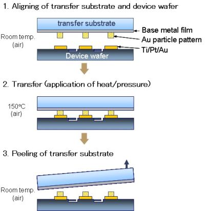
TOKYO, July 12, 2011 - (ACN Newswire) - Tanaka Kikinzoku Kogyo K.K.(1) and SUSS MicroTec KK will begin joint development of pattern transfer and bonding technology using sub-micron sized (1/10,000mm) gold particles.
 | | Tanaka Precious Metals and SUSS MicroTec to Jointly Develop Sub-micron Gold Particle Pattern Transfer and Bonding Technology |
This joint development will encompass development of technology for transferring patterns of sub-micron gold particles to a silicon wafer at one time at the low temperature of 150 degrees Celsius on an industrial high volume production basis. Using the transferred pattern of gold particles which have an effect on absorbing wafer surface roughness, it is possible to achieve metal-metal bonding on a wafer level at the low temperature of 200 degrees Celsius, which had been difficult by using conventional technology, with enabling high temperature resistance, high reliability hermetic seals and electrical connections.
Through the joint development, the two companies aim to begin sales of the transfer substrates and the transfer and bonding equipment in March 2012. By implementing the bonding technology in packaging and assembly processes, manufacturers of MEMS (micro electro mechanical systems) devices, LED (light emitting diode) chips and small-sized chip electronic components can form fine patterns on silicon wafers for sealing frames and electrodes at once without any waste and a 100% usage rate (the ratio of material that can be mounted on a product) of expensive gold material. This is expected to lower the effective cost of key processes.
Current technology
Technological development and practical application aimed at reduced size, improved functionality, improved performance and lead-free soldering are currently being accelerated in the advanced device industry. Manufacturers in this industry has formed complex patterns such as hermetic sealing frames and electrodes on wafers with metals such as gold and gold-tin by combining multiple patterning processes such as plating, screen printing and sputtering. This not only lowers rate of the production, but also decreases the efficiency of material utilization by going through several different processes and requires the reduction of material cost.
Furthermore, micro-bump bonding technologies such as gold bumps using plating and solder bumps are currently used in electrical connection processes, but these present issues such as the inability to obtain sufficient bonding stability because of hardness of gold bumps and unexpected contact by fluidity of molten solders. In addition, for hermetic sealing processes, technologies such as conventional anodic bonding and glass frit bonding, along with the recently developed metal-metal bonding using film deposition or plating are currently used, but the need for bonding at high temperatures and reduced yield caused by uneven surfaces have been issues.
Because of above issues, it is becoming difficult to meet all performance requirements such as high heat conductivity, high heat resistance, narrow line width and narrow pitch when using current technologies in the mounting of the latest devices such as high-brightness LEDs, which require stable operation at high temperatures.
Development of pattern transfer and bonding technology using sub-micron gold particles
In order to resolve such issues, through this joint development, precious metal material manufacturer Tanaka Kikinzoku Kogyo has developed manufacturing processes of a substrate for pattern transferring of sub-micron gold particles which offer higher heat resistance and lower stress than existing joints by soldering, and able to be bonded at low temperature due to its size effect. Meanwhile, SUSS MicroTec, which sells wafer bonding devices globally, will develop a wafer-level transfer and bonding equipment using such transfer substrates. This technology development is being carried out with the cooperation of Professor Shuichi Shoji and Associate Professor Jun Mizuno, Nanotechnology Research Laboratory, Waseda University.
The pattern transfer and bonding technology developed here enables electrical connections and hermetic seals with the minimum necessary amount of gold material while also resolving issues faced when using current technologies. It is perfect for the following manufacturing processes.
- Hermetic seals in advanced MEMS
- One-time processing of hermetic seals and electrical connections in advanced MEMS
- Formation of bump electrodes in devices operating at high temperatures, such as high-brightness LEDs and power semiconductors
- Formation of minute bump electrodes on small-sized chip electronic components
- 3D integration of wafers
Tanaka Kikinzoku Kogyo and SUSS MicroTec will have a joint booth at Exhibition Micromachine/MEMS 2011 held at Tokyo Big Sight (Ariake, Koto-ku, Tokyo) on July 13 (Wed.) -15 (Fri.), 2011. The booth (East Hall 2, B-05) will contain exhibits of samples of transfer substrate of sub-micron gold particle and substrate subjected to transferred patterns, and technical staff will be on-site to respond to interviews.
(1) Tanaka Kikinzoku Kogyo K.K.:
The core company conducting manufacturing operations in the Tanaka Precious Metals, which has TANAKA HOLDINGS Co., Ltd. as its holding company.
Company release, with images:
www.acnnewswire.com/clientreports/508/Tanaka_EN_712.pdf
About TANAKA HOLDINGS Co., Ltd. (Holding company of Tanaka Precious Metals)
Headquarters: 22F, Tokyo Building, 2-7-3 Marunouchi, Chiyoda-ku, Tokyo
Representative: Hideya Okamoto, President & CEO
Founded: 1885
Incorporated: 1918
Capital: 500 million yen
Consolidated employees: 3,441 (FY2009)
Consolidated net sales: 710.2 billion yen (FY2009)
Main businesses of the group: Manufacture, sales, import and export of precious metals (platinum, gold, silver, and others) and various types of industrial precious metals products. Recycling and refining of precious metals.
Website: http://www.tanaka.co.jp
About Tanaka Kikinzoku Kogyo K.K.
Headquarters: 22F, Tokyo Building, 2-7-3 Marunouchi, Chiyoda-ku, Tokyo
Representative: Hideya Okamoto, President & CEO
Founded: 1885
Incorporated: 1918
Capital: 500 million yen
Employees: 1,599 (FY2009)
Sales: 388.8 billion yen (FY2009)
Businesses: Manufacture, sales, import and export of precious metals (platinum, gold, silver, and others) and various types of industrial precious metals products. Recycling and refining of precious metals.
Website: http://pro.tanaka.co.jp
About the Tanaka Precious Metals
Established in 1885, the Tanaka Precious Metals has built a diversified range of business activities focused on the use of precious metals. On April 1, 2010, the group was reorganized with TANAKA HOLDINGS Co., Ltd. as the holding company (parent company) of the Tanaka Precious Metals. In addition to strengthening corporate governance, the company aims to improve overall service to customers by ensuring efficient management and dynamic execution of operations. Tanaka Precious Metals is committed, as a specialist corporate entity, to providing a diverse range of products through cooperation among group companies.
Tanaka Precious Metals is in the top class in Japan in terms of the volume of precious metal handled, and for many years the group has developed and stably supplied industrial precious metals, in addition to providing accessories and savings commodities utilizing precious metals. As precious metal professionals, the Group will continue to contribute to enriching people's lives in the future.
The eight core companies in the Tanaka Precious Metals are as follows.
- TANAKA HOLDINGS Co., Ltd. (pure holding company)
- Tanaka Kikinzoku Kogyo K.K.
- Tanaka Kikinzoku Hanbai K.K.
- Tanaka Kikinzoku International K.K.
- Tanaka Denshi Kogyo K.K.
- Electroplating Engineers of Japan, Limited
- Tanaka Kikinzoku Jewelry K.K.
- Tanaka Kikinzoku Business Service K.K.
About SUSS MicroTec K.K.
Head office: German Industry Park, 1-18-2 Hakusan, Midori-ku, Yokohama-shi, Kanagawa
Representative: Raymond Lau, Representative Director
Incorporated: 1988
Capital: 30 million yen (wholly-owned by SUSS MicroTec AG (Munich, Germany))
Employees: 25 / Consolidated group employees: 616 (as of FY2011)
Consolidated group sales: Euro 139.1 million
Areas of business: Development, sale and technical servicing of manufacturing equipments for MEMS and semiconductor industries
Products:
- Manual & Automatic Coater & Developers
- Manual & Automatic Mask Aligners
- Manual & Automatic Wafer Bonders
- Permanent & Temporary Wafer Bonders
- Photo Mask Manufacturing Equipments
Website: http://www.suss.com/jp.html
About SUSS MicroTec
SUSS MicroTec is a leading supplier of equipment and process solutions for microstructuring in the semiconductor industry and related markets. In close cooperation with research institutes and industry partners SUSS MicroTec contributes to the advancement of next-generation technologies such as 3D Integration and nanoimprint lithography as well as key processes for MEMS and LED manufacturing.
With a global infrastructure for applications and service SUSS MicroTec supports more than 8,000 installed systems worldwide. SUSS MicroTec is headquartered in Garching near Munich, Germany.
For more information, please visit http://www.suss.com .
Press inquiries
Tokyo Sales Dept., Tanaka Kikinzoku International K.K. (TKI)
E-mail: tki-contact@ml.tanaka.co.jp
SUSS MicroTec K.K.
Hiroyuki Ishida, Business Development Dept.
E-mail: h.ishida@suss.jp
Topic: Press release summary
Source: TANAKA PRECIOUS METAL GROUP Co., Ltd.
Sectors: Metals & Mining, Materials & Nanotech
https://www.acnnewswire.com
From the Asia Corporate News Network
Copyright © 2026 ACN Newswire. All rights reserved. A division of Asia Corporate News Network.
|
|
|
|

|
|
|
| |
| TANAKA PRECIOUS METAL GROUP Co., Ltd. Related News |
|
| Tuesday, 28 April 2026, 21:00 JST |
| TANAKA to Showcase Advanced Semiconductor Materials and Circular Economy Initiatives at SEMICON Southeast Asia 2026 |
|
| Thursday, 16 April 2026, 21:00 JST |
| TANAKA PRECIOUS METAL NEXT Certified as a Special Subsidiary |
|
| Mar 31, 2026 20:00 HKT/SGT |
| TANAKA Memorial Foundation Announces Recipients of Precious Metals Research Grants |
|
| Mar 20, 2026 20:00 HKT/SGT |
| TANAKA Announces Executive Appointments |
|
| Tuesday, 17 March 2026, 21:00 JST |
| TANAKA PRECIOUS METAL GROUP Provides Medals, Commemorative Items, and Trophies as Category Sponsor (Awards Ceremonies) for the LIGA.i Blind Soccer Top League 2025 |
|
| More news >> |
|
|
|

